Pulsed Laser Deposition
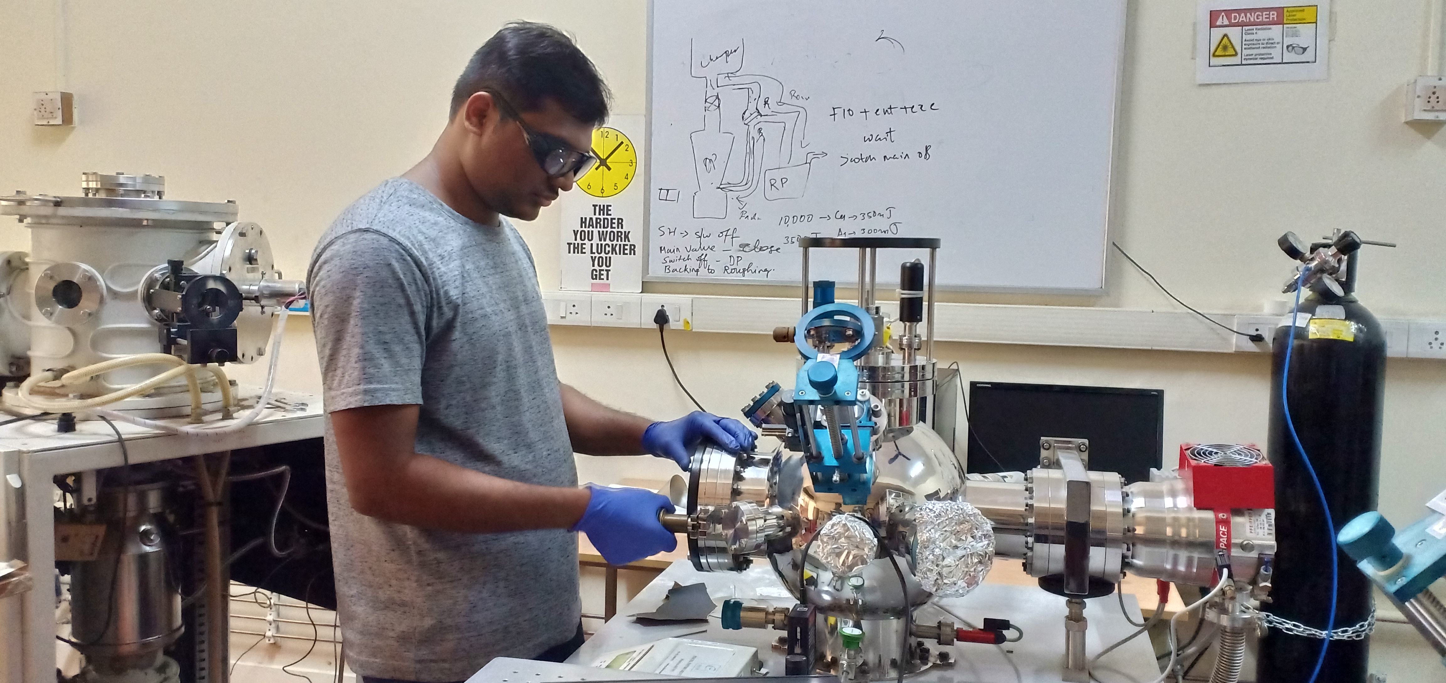
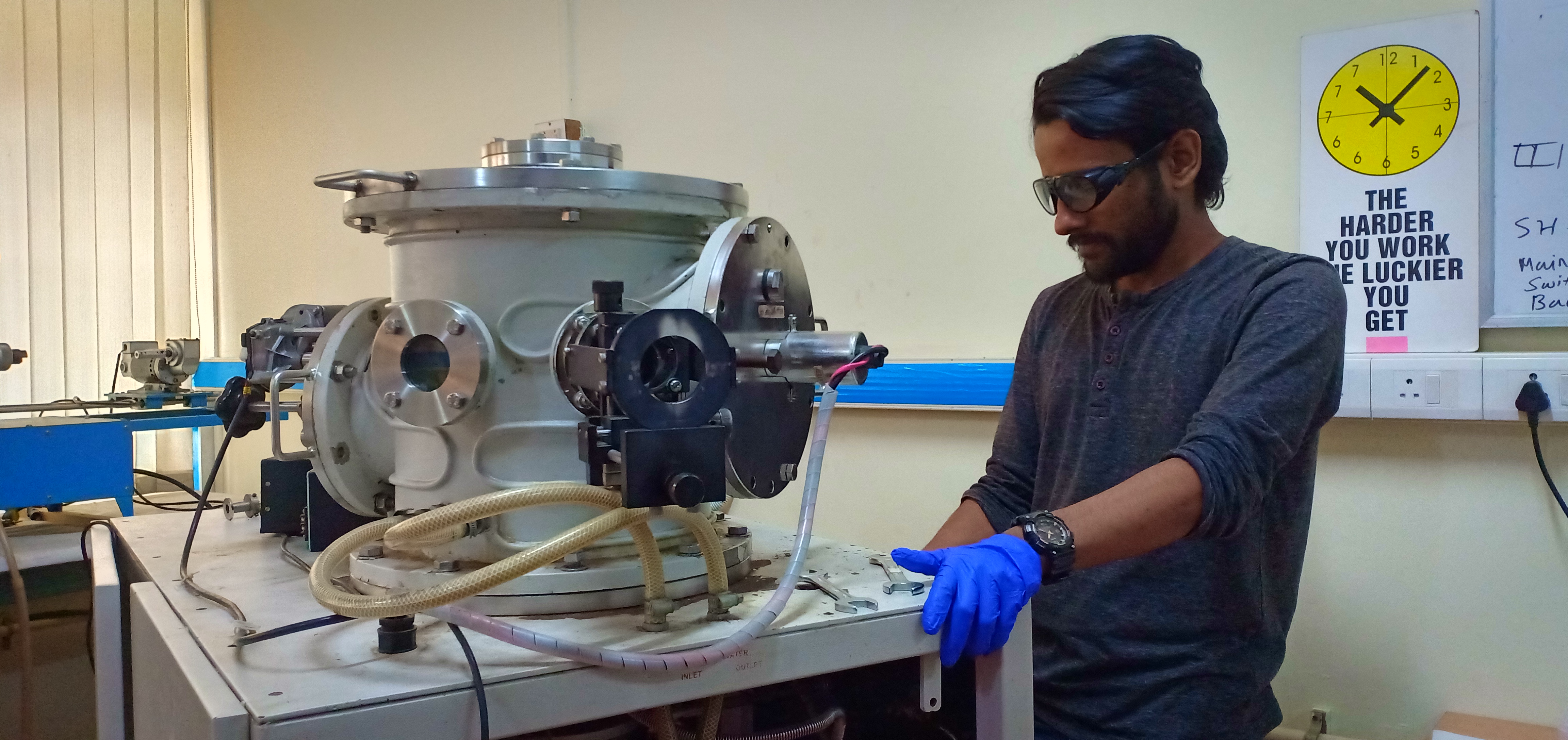
Pulsed laser deposition is a versatile technique to deposit high quality oxide thin films. This technique uses high power laser pulses (typically ~108 Wcm-2) to melt, evaporate and ionize material from the surface of a dense target. This "ablation" event produces a transient, highly luminous plasma plume that expands rapidly away from the target surface. The ablated material is collected on an appropriately placed substrate upon which it condenses and the thin film grows.
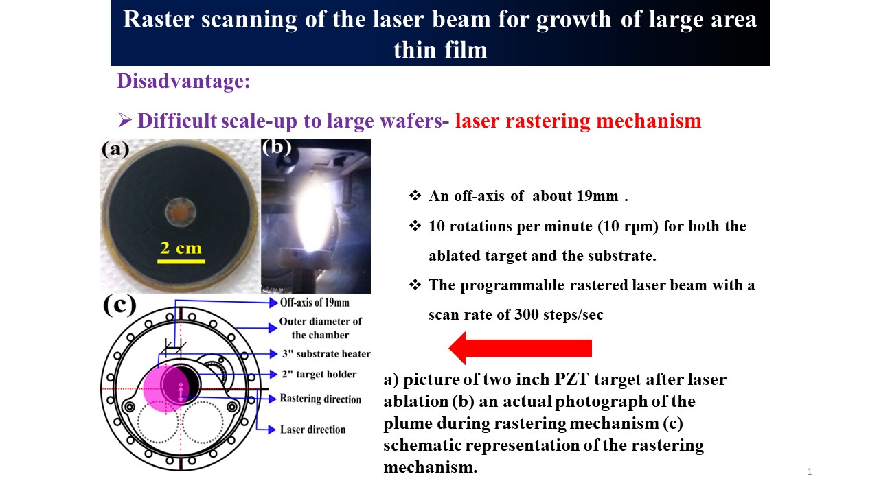
We have our state of art PLD facility (Excel instruments and Hind Hivac) in MSRC for different variety of oxide materials. We used to grow binary oxides to garnets using this technique. One of the draw backs of PLD is the limited area of deposaition, we have circumvented this issue by developing rsatering mechanism to deposit oxide thin films on large area(2 inch).Also we have a nano assisted pulsed laser deposition facility (NAPLD) to grow nano rods and quantum dots.
RF MAGNETRON SPUTTERING:
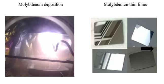
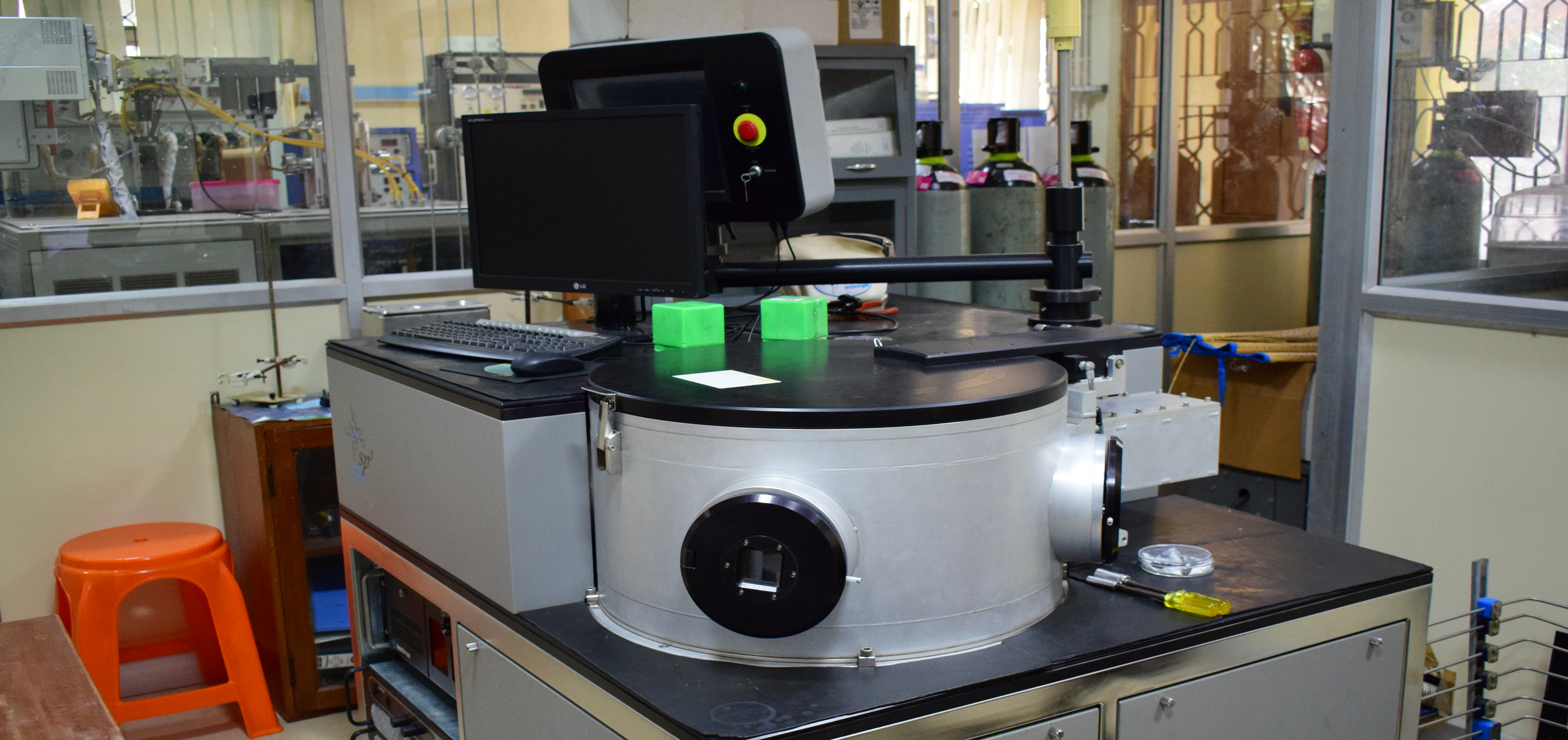
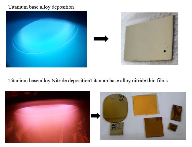
Sputtering is widely used PVD technique to deposit thin film onto the substrate. Sputtering process is based on generation of glow discharge between two electrodes in vacuum environment. The deposition chamber is evacuated to high vacuum ̴ 5x10, sputter gas typically inert gas such as Argon is introduced (in case of reactive sputtering gases such as Oxygen or Nitrogen is introduced along with Ar) in controlled amount as required. With sufficiently high potential difference between two electrodes the sputter gas (Ar) ionized and electrical discharge forms. These charged Ar ion are accelerated towards source material (cathode) hence momentum exchangedue to bombardment of high energetic particles (ions) to the surface of source material (target) leads to knocking off the surface atoms. These ejected atoms then travel towards substrate and eventually forms thin film.
In direct current (DC) sputtering of metals, negative potential is applied to the target which attracts the positive ion from the plasma (Ar+). These high energy positive ions bombard the target surface, knocking off the atoms from the surface and also captures the electron from target (metal surface). These ions then became neutral and drift from the target surface and became part of background gas and again involved in sputtering process.
If the target is a non-conducting material the positive charge will build up on the surface of target which eventually stops the sputtering process. Alternative current (RF or pulsed DC) sputtering is used to deposit both conducting and non-conducting materials.Materials such as oxides, nitrides, and ceramics have very large DC impedance and require prohibitively high voltages to ignite and maintain a plasma. However the impedance of these materials changes with the frequency of the applied power. Using power delivered at radio frequencies (RF) – typically at 13.56 MHz – and an automatic impedance matching network, the total impedance of the circuit can be regulated to reasonable low values which is suitable for plasma ignition in typical sputtering environments.Magnetron is added to accelerate the ionization processes as strong magnetic field provide long helical path for electron which causes cascaded collision between neutral Ar atom and electron, and enhance ionization process. This arrangement also confined the plasma close to the target which prevents the deposited thin film from damage due to high energetic particles of plasma.
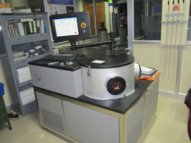
We have RF magnetron sputtering unit in our lab. Deposition can be done at room temperature and post annealing can be done up to 400˚C.
- Specifications:
- Target material: Metals, alloys, metal oxides, metal nitride.
- Target size: 2”, 5 mm
- Sputtering medium: Argon
- Reactive sputtering medium: Ar+O2, Ar+ N2
- Substrate: any substrate with flat surface, size- 2”x2”
- RF power: 50 to 500 W
- Ar / reactive gas pressure: 0.06 to 0.6 mbar
Hot Filament Chemical Vapour Deposition :-
- The name Hot Filament Chemical Vapor Deposition (HFCVD) is self-explanatory that hot filaments are being utilized to activate the carbon-containing precursor gases for the growth of diamond on the substrate.
- The Model 650 CVD Diamond Deposition System combines proven hot-filament reactor technology with advanced controls to produce superior polycrystalline diamond coatings. HFCVD system uses a vacuum chamber (12’’) continually pumped using a rotary pump, while process gases are metered in at carefully controlled rates.
- Throttle valves maintain the pressure in the chamber at typically 5-50 Torr, while a substrate is heated up to a temperature of 700 - 900 °C. The substrate to be coated sits on the holder, a few millimeters beneath a filament, which is electrically heated to temperatures in excess of 2200 °C.
- The patented Tungsten filament assembly generates uniform energy distribution which ensures the uniform diamond films over large area (12 inch diameter Si can be coated uniformly). Methane (CH4) diluted in excess of hydrogen (H2) (in a typical mixing ratio of 1%vol. CH4) is used as precursor gas.
- The Reactor offers high quality nano or micro-crystalline diamond films deposition on different substrates from Si, SiC, W, Ti etc... and non-planar diamond coating on cutting tools.
- A multi-step (up to 58 discrete steps), recipe-driven controller ensures repeatable coatings with optimum characteristics.
- The deposition process is controlled by thermal management of both filament and substrate temperatures, in conjunction with closed-loop pressure and gas flow control.
PHYSICAL VAPOUR DEPOSITION:
It includes variety of thin film deposition techniques where the solid material vaporized/ sublimate/ ablated in high vacuum environment and deposited on substrate. For thin films deposition all PVD techniques include three fundamental steps-
- Vaporization of the material from a solid source- resistive heating, laser ablation or gaseous plasma.
- Transportation of the vapour in vacuum or partial vacuum to the substrate surface.
- Condensation onto the substrate to generate thin films.
- Heating element- Tungsten filament/boat, Molybdenum boat.
- Source material- Aluminium, Gold.
- Base pressure- 2x10⁻⁵ mbar.
- Thickness- ̴ 50 to 500 nm.
THERMAL EVAPORATION:-
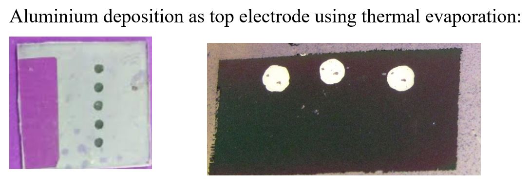
It is a PVD method to deposit elemental thin films on various substrate. In thermal evaporation solid material in heated to its melting point or sublimate (via resistive heating) in high vacuum chamber which evaporates the source material and produces some vapour pressure of it. This evaporated material is constitutes of vapour stream, which traverses from source to substrate and condensed as thin film.
We use thermal evaporation to make contacts on various lab level devices.
